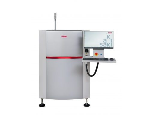
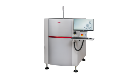
2Di-LU1 Bottom Side
Bottom-scan AOI system for automated PCB back-end production.
Ensure full traceability and Quality Assurance Data availability for back-end production. Prevent damage from manual or automated board handling by eliminating the need to flip the PCBs.
SAKI’s unique Line Scan imaging technology is applied to bottom-side inspection. High-speed imaging enables inspection of large PCBs in one pass in about 9 seconds. The newly developed high-rigidity conveyor is compatible with large odd-shaped inserted component mounted-PCBs and heavy jigs. Covering the scanner with tempered glass protects it against falling flux and foreign substances. It provides easy maintenance and cleaning.
| Category | 2D AOI |
|---|---|
| Our solution | Inspection in SMT |
| Supplier | Saki |
Main features and benefits of the device
- Unique Fujiyama algorithm verifies five critical aspects of through-hole solder joints
- Simultaneous inspection of the following defects: copper exposure, excessive solder, pin presence, insufficient solder, blow holes, solder bridges
- Detection of unexpected defects such as: plastic mold chipping, dropped chip parts, reel tape fragments, foreign substances, PCB pattern defects, solder frame damage
- SAKI’s Line Scan technology scans the entire PCB in one pass
- Extra Component Detection (ECD) inspection capability
- Offline programming
Write to us, we will be happy to answer your questions and find a solution for you.
Related categories
Matrix Technologies GmbH is a global supplier of high-speed Automated Inline X-ray Inspection systems (AXI) and semi-automated X-ray Inspection...
We offer a range of 2D and 3D X-ray devices for microfocal inspection of electronics. The devices of the German manufacturer YXLON are defined...
We offer 3D AOI (Automatic Optical Inspection) produced by the company Saki Corporation. The Saki AOI machines are unique with their 3D technology...
